|
POWER2/P2SC Processor
SG24-4810-00 Understanding IBM RS/6000 Performance and Sizing
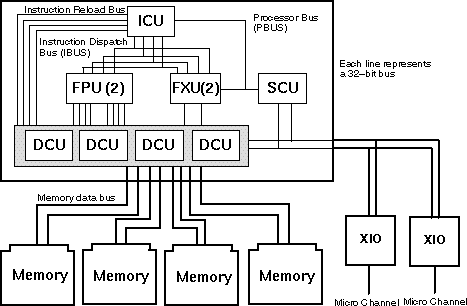
The early POWER2 processor complex consists of eight semi-custom
chips partitioned in the same way as the POWER: the instruction cache unit
(ICU) which also processes branches, the FXU, FPU, four data cache units
(DCUs), and a storage control unit (SCU). The early models of the POWER2
were announced in September 1993 and are the basis of the POWER2 Super
Chip (P2SC) version. The POWER2 architecture expands the cache capacity,
doubles the number of
functional units, doubles the bandwidth of most buses, and quadruples
the cache to floating-point bandwidth.
The POWER2 architecture offers numerous performance gains:
· New instructions enhance floating-point bandwidth, square
root, and data conversion.
· User-level instruction set is a superset of the original POWER
set. Existing POWER binaries can
run unmodified on the faster systems.
· Existing POWER binaries gain the performance benefits of the
larger data cache, higher clock
rates, improved bandwidth, and additional
functional units.
· Recompiling can maintain portability while providing gains
from added compiler transformations
. When portability is not required, a recompiled application
can also exploit new instructions.
POWER implements one floating-point, one integer, and one
branch unit. It can execute four instructions per cycle (five operations).The
POWER2 multichip implements dual integer, floating-point, and branch units
that can execute six instructions per cycle (eight operations).
The architecture features high-performance, floating-point
storage access instructions, load quad word (128 bits) and store quad word,
which support all of the addressing forms of double-precision storage references.
The load quad word moves two adjacent double-precision storage operands
into two adjacent floating-point registers.
The instruction cache size is 32 KB, two-way set associative,
and the data cache is either 128 KB or 256 KB, four-way set associative
single line, depending on the RS/6000 model. The following are some other
differences in the POWER2 multichip compared to the POWER architecture:
· Eleven new instructions (giving a total of 195 instructions)
· Different page frame table format (hash instead of inverted
page frame tables)
· Page aliasing
· Support for floating-point imprecise mode
· Different interrupt mechanism
· Faster clock speed
· Doubles B/W from memory to scache (eight-word bus, 128 bytes)
· Double B/W from scache to sinteger (two single words,16 bit)
and FPUs (two quad words, 32 bit)
· Different alignment requirements for the quad word data
· A special data address break-point register
· A performance monitoring facility
Figure 13. POWER2 Eight-Word System

ICU Instruction Cache Unit
FXU Fixed Point Unit
FPU Floating Point Unit
DCU Data Cache Unit
SCU Sorage Control Unit
POWER2 Super Chip
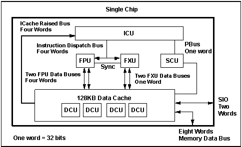
The POWER2 Super Chip (P2SC) is a compression of the POWER2
eight-chip architecture into a single chip with increased processor speed
and performance. It retains the design of its predecessor, the POWER2.
The initial models have clock speeds of 120 MHz and 135 MHz.
High-density CMOS-6S technology allows each to incorporate 15 million transistors.
The most significant change is a halving of the size of the data cache
and the data TLB, which now are 128 KB and 256 KB, respectively. These
changes were required to fit the eight-chip processor onto a single chip.
The P2SC delivers the processing and dual floating-point
power needed for large, numeric-intensive tasks as well as the integer
and transaction performance for commercial applications. The P2SC contains
on-chip 32 KB instruction and 128 KB data cache and is full binary compatible
with the POWER2 architecture.
Figure 14. POWER2 Super Chip Module

ICU Instruction Cache Unit
FXU Fixed Point Unit
FPU Floating Point Unit
DCU Data Cache Unit
SCU Sorage Control Unit
The P2SC can issue and execute six instructions per cycle,
two of which can be floating-point multiply-add (FMA) instructions. It
supports register renaming and out-of-order execution, although only for
floating-point instructions. With dual branch units, the P2SC can also
execute two branches per cycle, although only one can be taken, while the
other is put on hold. The data cache is triple-clocked to handle two CPU
accesses (load or store) plus a cache refill (write to cache from main
memory). Thus, this part of the chip operates at 500 MHz.
The P2SCs great performance is directly associated with
the inclusion of up to 2 GB of DRAM across a 256-bit-wide interface. This
interface plugs the processor directly into a byte stream bus of up to
2.2 GB per second. The chip also integrates a 64-bit I/O bus for peripheral
interconnection.
>Can anyone tell me when where the MicroChannel Bus bottlenecks on
the RS/600 line?
Milton Miller
For the Combo boxes (520-560 except 550L, 320-340 and 350, 920, 930),
the Micro Channel and IOCC max out about 17MB/s (writes) and 19MB/s (reads).
The newer XIO IOCC mahcines (Power w/32k I-cache and POWER2 machines) max
out at 77MB/s (read or write per bus) sustained. These are based
on long (4k) block transfers by Bus Master devices, smaller blocks, slower
adapters, and PIO to initate transfers will lower achieved throughput.
Also, in Combo boxes PIO (loads and stores vs dma) had last priority,
in XIO they are hidden under grant (highest priority).
> (which models use the bus for memory access?)?
All the RS/6000 series (including the PowerPC boxes) have a bridge
from the IO bus to a system bus which gives access to memory for DMA (none
use the Micro Channel for system memory).
In systems with dual Micro Channel busses, both buses can operate at
full bandwidth at the same time
Faster XIO instead of I/O Channel Controller IOCC (Micro Channel
controller)
Frank Kraemer
>IBM ALSO has a link which IS proprietary called Serial Optical. This
link hangs DIRECTLY OFF the CPU ( as opposed to all of the other network
types which run via the Micro-channel ). It is this serial optical link
that IBM itself uses to create parallel computing arrangements of RS/6000s.
Serial Optical is only available on certain models of RS/6000. I think
it is: 930,970,980,560, and 580 - maybe 540 & 550 also have it - I
can't remember.
Serial Optical Link (called SOCC) IS proprietary - YES, but it's driven
from the IOCC (I/O Controller Chip). The IOCC is attached to the CPU/RAM
channel and drives the MicroChannel bus and the SOCC ports. It offers about
twice the FDDI speed and is very very cheap, yes I know IBM and cheap are
two different words ;-), but it's true. One SOCC adapter has two ports.
You can have 1 SOCC adapter in all 5xx systems (2 ports) - all 9xx systems
support 1 SOCC adapters (4 ports). The SOCC adapter does not need a MicroChannel
slot.
+--------+
+--------+
! CPU ! =========================!
RAM !
+--------+
!!
+--------+
!!
!!
40 MB/s MC or !!
80 MB/s MC +--------+
SOCC !--- SOCC Port 1
+--------!
IOCC ! =======+
(220 Mbit/s)
!
+--------+ !--- SOCC Port
2
!
!
+------
Micro Channel ......
!
+------
Micro Channel ......
!
+------
Micro Channel Adapter for FDDI (100 Mbit/s)
!
+------
.....
The main disadvantage of SOCC is the point to point connection. Without
any special switch you can connect only 3 boxes (5xx) together. This is
a good solution for some kind of compute cluster,
but if you think of clustering more boxes the NSC switch is big money.
So the best solution is the combination of SOCC and FDDI:
....===================================....FDDI/Ethernet/TR
! !
!
X X
X
/
\ / \
/ \
/ 1 \
/ 2 \ / 3 \
SOCC clusters 1,2,3
X-----X
X-----X X-----X
!
! ! !
! !
....=====================================...FDDI/Ethernet/TR
before I stop, SOCC runs TCP/IP....
9595 Main Page
|

